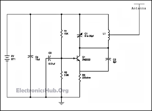
Friday, 14 February 2014

2 km FM transmitter


2 km FM transmitter


Description.
With a matching antenna, the FM transmitter circuit shown here can transmit signals up to a range of 2 kilo meters. The transistor Q1 and Q2 forms a classic high sensitive preamplifier stage. The audio signal to be transmitted is coupled to the base of Q1 through capacitor C2. R1, R3, R4, R6, R5 and R9 are the biasing resistors for the preamplifier stage comprising of Q1 and Q2. Transistor Q3 performs the collective job of oscillator, mixer and final power amplifier.C9 and L1 forms the tank circuit which is essential for creating oscillations. Inductor L2 couples the FM signal to the antenna.
Circuit diagram.
2km Fm transmitter
Notes.
  • Assemble the circuit on a good quality PCB.
  • The circuit can be powered from anything between 9 to 24V DC.
  • Inductor L3 can be a VK220J type RFC.
  • For L1 make 3 turns of 1mm enamelled copper wire on a 10mm diameter plastic former. On the same core make 2 turns of 1 mm enamelled copper wire close to L1 and that will be L2.
  • Frequency can be adjusted by varying C9.
  • R9 can be used to adjust the gain.
  • For optimum performance, value of C8 must be also adjusted.
  • Using a battery for powering the circuit will reduce noise.

Sunday, 9 February 2014

simple FM transmitter

                simple FM transmitter

Here, is a very interesting and simple project in the series of communication used to transmit noise free F.M. signal in the wide range up to 100 M using only one transistor. The transmitted message from F.M. transmitter circuit is received by the receiver having the facilities of F.M. channel or you can also try F.M. receiver circuit published in this website.

Circuit Description of simple F.M. transmitter

The entire circuit of F.M. transmitter is divided into three major stage i.e. oscillator, modulator and amplifier. The transmitting frequency of 88-108 MHz is generated by adjusting VC1. The input voice given to microphone is changed into electric signal and is given to base of transistor T1. Transistor T1 is used as oscillator which oscillates the frequency of 88-108 MHz. The oscillated frequency is depended upon the value R2, C2, L2 and L3. This transmitted signal from F.M. transmitter is received and tuned by F.M. receiver.
simple and powerful f.m. transmitter

PARTS LIST

Resistors (all ¼-watt, ± 5% Carbon)
R1 = 180 KΩ
R2 = 10 KΩ
R3 = 15 KΩ
R4 = 4.7 KΩ

Capacitors

C1 = 10 KPF
C2 = 10 PF
C3 = 20 KPF
C4 = 0.001 µF
C5 = 1 µF/10V
C6 = 4.7 PF
C7 = 10 KPF
C8 = 3.3 PF
VC1 = 22 PF

Semiconductor

T1 = BF194B

Miscellaneous

MIC1 = Condenser mike
L1, L2 = 3 turns of 22 SWG wire around any thin pencil
L3 = 2 turns of 22 SWG wire around any thin pencil.


Walky-talky without using inductor or coil


Walky-talky without using inductor or coil


Walky-talky in this website is world 1st verified walky-talky project without using coil. Walky talky is very interesting and attain grabbing project for electronics hobbyist. Communication is done without any physical connection and mobile network up range of 500 meter. Almost all communication devices utilize coil which is burden for electronics hobbyist. So, we design this circuit without using any coil.

Circuit Descriptions of walky-talky

The entire circuit of walky-talky is divided into two main section transmitter and receiver section.
Transmitter section:- Transmitter section utilize  IC NE566 (IC4) as VCO (Voltage Control Oscillator) for generating frequency about 30 KHz. Resistor R24 with Capacitor C24 used as frequency components for frequencies determination. Voice is pick-up by mike (MIC1) and changed it into equivalent electrical signal. Signal from microphone is amplified by transistor T4 and given to pin no 5 0f IC4. NAND gate N1 with crystal oscillator XT4 finalizes the output from pin 3 of IC3. Lastly, signal from NAND N2 through N3 and N4 given to antenna for transmission.
Receiver section: - Transmitted signal from another walky-talky is received from same antenna which is used for transmission. Field effect transistor T1 boosts the received signal and make more powerful and send to amplifier section made from transistor T2 and T3 with crystal oscillator XT1 through XT3. Detector section is made from diode D1, Capacitor C6 and resistor R12. 30 KHz frequency is obtained from detector section.
Frequency of Phase Locked Loop IC NE565 (IC1) is adjusted by capacitor C9, resistor R17 and variable resistor VR1. Amplifier IC LM386 (IC2) is used to amplify the signal and given to speaker.

PARTS LIST

Resistors (all ¼-watt, ± 5% Carbon)
R1 = 47 KΩ
R2 = 100 Ω
R3, R4, R11, R27 = 2.2 KΩ
R5 = 330 KΩ
R6, R10 = 560 Ω
R7 = 1 KΩ
R8 = 220 KΩ
R9 = 100 Ω
R12, R15, R16 = 4.7 KΩ
R13, R31 = 10 KΩ
R14 = 15 KΩ
R17 = 1.8 KΩ
R18 = 1.2 KΩ
R19 = 1 KΩ
R20 = 4.7 Ω
R21, R22 = 100 KΩ
R23 = 120 KΩ
R24 = 5.6 KΩ
R25 = 22 KΩ
R26 = 150 KΩ
R28 = 330 Ω
R29 = 220 KΩ
R30 = 47 KΩ
VR1 = 4.7 KΩ
VR2 = 22 KΩ

Capacitors

C1, C6, C10, C24 = 1 KpF
C2, C4, C5 = 47 KpF
C3 = 20 KpF
C7, C9, C23= 2.2 KpF
C8 = 4.7 µF/16V
C11 = 22 KpF
C12, C16 = 0.1 µF
C13 = 2.2 µF/16 V
C14, C19, C25, C26 = 0.22 µF
C15 = 10 µF/16V
C17 = 220 µF/16V
C18, C20 = 10 KpF
C21, C22 = 68 pF
C27 = 1000 µF/16V
C28 = 10 µF/16V

Semiconductors

IC1 = NE565 (Phase Lock IC)
IC2 = LM386 (Amplifier IC)
IC3 = CD4011 (Quad 2-input NAND Gate IC)
IC4 = LM566 (Voltage Controlled Oscillator)
IC5 = LM7812 (Voltage Regulator)
T1 = BFW10
T2, T3 = BF194
T4 = BC148
D1 = 1N4148

Miscellaneous

XT1 – XT4 = 10.7 MHz crystal
SW1 = Single pole double throw switch
LS1 = 8Ω speaker
MIC1 = Condenser microphone
Areal

Saturday, 8 February 2014

Varying brightness AC lamp

Varying brightness AC lamp

In this circuit, an SCR is used to slowly vary the intensity of a 120 volt light bulb by controlling the time that the AC line voltage is applied to the lamp during each half cycle.

Caution:

The circuit is directly connected to the AC power line and should be placed inside an enclosure that will prevent direct contact with any of the components. To avoid electrical shock, do not touch any part of the circuit while it is connected to the AC power line. A 2K, 10 watt power resistor is used to drop the line voltage down to 9 volts DC. This resistor will dissipate about 7 watts and needs some ventilation.

Operation:

A couple NPN transistors are used to detect the beginning of each half cycle and trigger a delay timer which in turn triggers the SCR at the end of the delay time. The delay time is established by a current source which is controlled by a 4017 decade counter. The first count (pin 3) sets the current to a minimum which corresponds to about 7 milliseconds of delay, or most of the half cycle time so that the lamp is almost off. Full brightness is obtained on the sixth count (pin 1) which is not connected so that the current will be maximum and provide a minimum delay and trigger the SCR near the beginning of the cycle. The remaining 8 counts increment the brightness 4 steps up and 4 steps down between maximum and minimum. Each step up or down provides about twice or half the power, so that the intensity appears to change linearly. The brightness of each step can be adjusted with the 4 resistors (4.3K, 4.7K, 5.6K, 7.5K) connected to the counter outputs. The circuit has been built by Don Warkentien (WODEW) who suggsted adding a small 47uF capacitor from ground to the junction of the current source transistor (PNP) to reduce the digital stepping effect so the lamp will brighten and fade in a smoother fashion. The value of this capacitor will depend on the 4017 counting rate, a faster rate would require a smaller capacitor.

120 VAC Lamp Dimmer

120 VAC Lamp Dimmer

The full wave phase control circuit below was found in a RCA power circuits book from 1969. The load is placed in series with the AC line and the four diodes provide a full wave rectified voltage to the anode of a SCR. Two small signal transistors are connected in a switch configuration so that when the voltage on the 2.2uF capacitor reaches about 8 volts, the transistors will switch on and discharge the capacitor through the SCR gate causing it to begin conducting. The time delay from the beginning of each half cycle to the point where the SCR switches on is controlled by the 50K resistor which adjusts the time required for the 2uF capacitor to charge to 8 volts. As the resistance is reduced, the time is reduced and the SCR will conduct earlier during each half cycle which applies a greater average voltage across the load. With the resistance set to minimum the SCR will trigger when the voltage rises to about 40 volts or 15 degrees into the cycle. To compensate for component tollerances, the 15K resistor can be adjusted slightly so that the output voltage is near zero when the 50K pot is set to maximum. Increasing the 15K resistor will reduce the setting of the 50K pot for minimum output and visa versa. Be careful not to touch the circuit while it is connected to the AC line.

Lamp Flasher using NE 555


Flasher Circuit using NE 555

Description


This is the circuit diagram of lamp flasher operated from mains. By this you can flash up to 200 Watt lamps at rates determined by you. IC NE555 is wired as an astable multivibrator for producing the pulses for flashing the lamp. The flashing rate can be set by the value of resistors R2 & R3.
Diodes D1 & D2 provides a half wave rectified regulated supply for the IC. Transistor T1 is used to drive triac and triac BT136 for driving the load. Resistor R4 limits the base current of Q1.

Flashing Circuit Diagram & Parts List

lamp-flasher12.jpg

Notes

  • Assemble the circuit on a good quality PCB or common board.
  • Connect a 100K pot instead of R2 if you need frequent changes in rate.
  • Many parts of the circuit are live with potential shock hazards.So please be careful.
  • As usual use an IC holder for mounting the IC.

        Modified Circuit

Lamp Flasher Circuit Using 555 Timer

Hi Fi Amplifier circuit


Hi Fi Amplifier Circuit – 2X12 Watts

Description.

Here is the circuit of a 2X12 watt H iFi  amplifier circuit using IC TDA 2616 from Phillips.A quiet simple and robust circuit using very less components.This makes the circuit ideal for a portable power amplifier.The circuit delivers 12 Watts power on  8 Ohm speaker for each channel at +/- 12 V dual supply.
The TDA2616 is a  stereo power amplifier IC comes  in a 9-lead single-in-line (SIL9) plastic power package (SOT131). This IC is  specially designed for mains fed amplifier circuits, such as stereo radio,tape  and television .The IC has good gain balance of both channels and Hi-fi in accordance with IEC 268 and DIN 45500 standards.Also the IC TDA 2616 has special inbuilt circuit for the  suppression of noise signals at the inputs, during switch-on and switch-off.This prevents click sounds during power on and power off.

Hi Fi Amplifier Circuit Diagram with Parts List.

Hi Fi Amplifier Circuit Schematic
           
                                 Hi Fi Amplifier Circuit Diagram

Notes.

  • All capacitors except C10 & C9 are ceramic.
  • All capacitors must be rated 50V.
  • Use a well regulated and filtered +/- 12 V dual power supply that is able to provide at least 2 A continuous current.


TDA 2616 Pin assignment & layout.

TDA 2616 PIN Description

                  TDA 2616 PIN Diagram and Configuration
  

We have more Audio Circuits in our website, that you may like to read;
1. Low Cost Amplifier
2. 50 Watt Transistor Amplifier
3. 3 Band Graphic Equalizer
4. Sound Shifter Circuit
5. Speech Amplifier Circuit

Night security light


Night security light


Description.

 Here is a simple circuit switches on a light around 2 hours after midnight, the time at which most of the robberies taking place.
This simple circuit is build around a CMOS IC 4060 to obtain the required timing. During day time the LDR has low resistance and keeps the pin 12 of the IC1 high, preventing the IC1 from oscillating. When it is dark the LDR resistance becomes high and the pin 12 of IC1 becomes low and the IC starts oscillating, which indicated by the flashing of LED D3.The values of the timing components R1, R2, C4 are so selected that the out put pin3 of IC1 goes high after 8 hours. That means the high output drives the triac to switch on the lamp around 2’O clock. At morning, the LDR resistance drops and the pin 12 of IC1 goes high and stops the oscillation, making the lamp OFF. The switch S1 can be used to manually ON the lamp. The capacitor C2 prevents false triggering.

Circuit diagram with Parts list.
night-security-light


Notes.
  •  Assemble the circuit on a good quality PCB or common board.
  • The LDR can be general purpose LDR.
  • The light sensitivity can be adjusted using the preset R6.
  • The IC1 must be mounted on an IC holder.

Audio monitoring system


Audio monitoring system


Description.
Here is the circuit schematic of a simple audio surveillance system in which the transmitter will pickup sound from one location and the receiver at other location will reproduce it. The receiver and transmitter are connected by only one set of wire. Here both power supply and transmitted signal share the same wire.
The audio signals picked up by the microphone will be amplified by the double stage amplifier build around transistors Q1 and Q2.The POT R2 controls gain of the amplifier. The power supply for this circuit is drawn from the interconnection lines itself. The capacitor C4 bypasses all audio frequencies & noise from the line and ensures pure DC for the circuit. The output of the amplifier (audio signal) is coupled to the line via the capacitor C6.
At the receiver end the capacitor C7 extracts the audio signal from the line and feds it to the inverting input of IC1 (TL071) which is wired as a voltage amplifier. Output of IC1 is given to the input of IC2 (LM386) which is a integrated power amplifier.IC2 provided necessary current gain to drive the speaker. The POT R14 can be used control the gain of receiver. Capacitor C11 isolates audio frequencies and noise from the power supply of both the ICs.
Circuit diagram with Parts list.


audio-monitoring-system-receiver
audio-monitoring-system-transmitter


Notes.
  • Assemble the circuit on a general purpose PCB.
  • Terminal A must be connected to A’ using the wire of required length. Do the same with B, B’.
  • The microphone M1 can be a general purpose one.
  • The speaker k1 can be 8 Ohm/2 Watt.
  • POT R2 can be used to control gain of the transmitter.
  • POT R14 can be used to control gain of the receiver.
  • The circuit can be powered from a 12V battery or 12V DC power supply.
  • IC1 and IC2 must be mounted on holders.

100W MOSFET power amplifier


  100W MOSFET power amplifier
A 100W MOSFET power amplifier circuit based on IRFP240 and IRFP9240 MOSFETs is shown here. The amplifier operates from a +45/-45 V DC dual supply and can deliver 100 watt rms into an 8 ohm speaker and 160 watt rms into a 4 ohm speaker. This Hi-Fi amplifier circuit is suitable for a lot applications like general purpose amplifier, guitar amplifier, keyboard amplifier. The amplifier can be also used as a sub woofer amplifier but a subwoofer filter stage has to be added before the input stage. The amplifier has a low distortion of 0.1%, a damping factor greater than 200, input sensitivity of 1.2V and the bandwidth is from 4Hz to 4 KHz.

Circuit diagram.

mosfet power amplifier
100W mosfet power amplifier circuit

About the circuit.

Capacitor C8 is the input DC decoupling capacitor which blocks DC voltage if any from the input source. IF unblocked, this DC voltage will alter the bias setting s of the succeeding stages. Resistor R20 limits the input current to Q1 C7 bypasses any high frequency noise from the input. Transistor Q1 and Q2 forms the input differential pair and the constant current source circuit built around Q9 and Q10 sources 1mA. Preset R1 is used for adjusting the voltage at the output of the amplifier. Resistors R3 and R2 sets the gain of the amplifier. The second differential stage is formed by transistors Q3 and Q6 while transistors Q4 and Q5 forms a current mirror which makes the second differential pair to drain an identical current. This is done in order to improve linearity and gain. Power amplification stage based on Q7 and Q8 which operates in the class AB mode. Preset R8 can be used for adjusting the quiescent current of the amplifier. The network comprising of capacitor C3 and resistor R19 improves high frequency stability and prevents the chance of oscillation. F1 and F2 are safety fuses.

Circuit setup.

Set R1 at midpoint before powering up and then adjust it slowly in order to get a minimum voltage (less than 50mV0 at the output. Next step is setting up the quiescent current and keep the preset R8 in minimum resistance and connect a multimeter across points marked X & Y in the circuit diagram. Now adjust R8 so that the multimeter reads 16.5mV which corresponds to 50mA quiescent current.

Notes.

  • Assemble the circuit on a good quality PCB.
  • Use a +45/-45 V DC, 3A dual supply for powering the circuit.
  • Power supply voltage must not exceed +55/-55 V DC.
  • Before connecting the speaker, check the zero signal output voltage of the amplifier and in any case it should not be higher than 50mV. If it is higher than 50mV, check the circuit for any error. Replacing Q1, Q2 with another set could also solve the problem.
  • Fit Q7 and Q8 to a 2°C/W heat sink. Both Q7 and Q8 must be isolated from the heat sink using mica sheets. Heat sink mounting kits for almost all power transistors/ MOSFETs of almost all package styles are readily available in the market.
  • All resistors other than R10, R11 and R19 are 1/4 watt metal film resistors. R10 and R11 are 5W wire wound type while R19 is a 3W wire wound type.

Power supply for the 100W MOSFET power amplifier.

+45/-45 dual supply mosfet amplifier
+45 / -45 dual supply for the 100W mosfet power amplifier
A basic dual power supply is used for the amplifier circuit. If 6A ampere bridge is not available, then make one using four 6A6 diodes.C10 and C11 are high frequency bypass capacitors. Filter capacitors C8 and C9 must be at least 10000uF, higher the value lesser the ripple. Optional 3A fuses can be added to the +45 and -45 lines. Transformer T1 can be a 230V primary, 35-0-35 V secondary, 300VA step down transformer.

TDA7294 100W Audio Amplifier


TDA7294 100W Audio Amplifier

100W Audio Amplifier TDA7294.

TDA7294 is an integrated, monolithic, Class AB audio amplifier designed specifically for Hi-Fi applications. The IC has a DMOS output stage and can deliver 100W RMS into an 8Ohm speaker at +/-38V dual supply. The TDA7294 has low noise, low distortion, good ripple rejection and can be operated from a wide range of supply voltages. The IC has built in short circuit protection and thermal shutdown circuitries. The IC is available in multiwatt 15V and multiwatt 15H packages.

Description.

In the circuit TDA7294 is configured to provide 100W output power into an 8Ohm loudspeaker at +/- 38V supply. C8 is the input coupling capacitor and the input is applied to the non-inverting input (Pin3) of the IC. C3 and C9 are power supply filter capacitors while C10 and C4 are bypass capacitors. C2 is the bootstrap capacitor. RC network comprising of R1 and C1 improves the high frequency stability of the amplifier and also prevents oscillations. R2 and C6 sets the mute time constant while R3 and C5 sets the standby time constant. S1 and the mute switch and S2 are the standby switch. R5 is the input resistance and the amplifiers input impedance has a direct relationship to its value. R4 and R6 is used for setting type closed loop gain and with the used value, gain is 30dB. C2 is a feedback capacitor and it also provides DC decoupling.

Circuit Diagram.

100W amplifier TDA7294
TDA7294 100W amplifier

Notes.

  • The supply voltage range is +/- 10V to =/-40V DC.
  • Heat sink is required and its thermal resistance should be around 0.038 degree Celsius/Watt.
  • Use an 8 Ohm 150W speaker as the load.
  • For 100W output the supply voltage must be +/-38VDC.
  • The power supply must be well filtered and free of ripples.
  • If ripples are present in the power supply it may cause oscillations.
  • VM = 1.5V is the mute ON threshold and VM=3.5V is the mute OFF threshold.
  • VSTBY = 1.5V is the standby on threshold and VSTBY = 3.5V is the standby OFF threshold.
  • Typical input resistance of TDA7294 is 100KiloOhm.
  • Frequency response is 20Hz to 20KHz.
  • 145 degree Celsius is the threshold for thermal shutdown. Slew rate of TDA7294 is 10V/microsecond and the open loop voltage gain is 80 dB.
  • Quiescent current of TDA7294 is approximately 30mA and its maximum value is 65mA.

60 watt amplifier circuit

60 watt amplifier STK4038.

STK4038 is an integrated AF power amplifier that can deliver 60 watts of output power into a 4 ohm load. The internal fixed current circuitry reduces switch ON/OFF clicks. The IC supports the addition of external circuits for thermal shutdown, pop noise reduction, output short circuit protection etc.

Description.

The 60 watt amplifier shown below is designed based on the datasheet and performs very well. Capacitor C1 is the input DC decoupling capacitor which blocks any DC level present in the audio input and C12 is the input by-pass capacitor. R1 is the input resistor.C10 and C8 are the ripple filter capacitors for the positive and negative power supply rails. R9 and R7 are the current limiting resistors for the internal driver stage while C11 and C3 are their corresponding filter capacitors. Resistor R6 feeds back a portion of the output signal to the inverting input (pin2). Gain of the amplifier depends on the value of R6. C9 and R2 forms a Zobel network which improves the high frequency stability of the amplifier.

Circuit diagram.

60W amplifier
60 watt amplifier circuit

Notes.

  • A good quality PCB improves the performance of the circuit.
  • Maximum supply voltage for STK4038 is +/- 57V DC.
  • K1 is a 4 ohm / 75 watt loud speaker.
  • While using 4 ohm speaker as the load, the power supply must not exceed +/- 32V DC.

Audio oscillator circuit


Audio oscillator circuit

ICL 8038 waveform generator.

ICL8038 is a monolithic waveform generator IC that can produce sine, square and triangular waveforms with very little distortion. The frequency can be programmed from 0.001Hz to 300 KHz using external timing capacitor and resistor. Frequency modulation and sweeping can be attained by using an external voltage. Other features of the ICL8038 are high linearity, high level outputs, simultaneous sine, square, triangle wave outputs, low external parts count, high temperature stability etc.
The working of ICL8038 is as follows. The external timing capacitor (C2 in the circuit diagram) is charged and discharged using two internal current sources. The first current source is on all the time and second current is switched ON and OFF using a flip-flop. Suppose the second current source is OFF and the first current source is ON, then the capacitor C2 will be charged with a continuous current (i) and the voltage across C2 increases linearly with time. When the voltage reaches 2/3 supply voltage, controlling flip flop is triggered and the first current source is activated. This current source carries double the current (2i) making the capacitor C2 is discharged with a current i and the voltage across it drops linearly with time. When this voltage reaches 1/3 supply voltage, the flip flop is resetted to the initial condition and the cycle is repeated again.

Circuit diagram – ICL8038 audio oscillator.

audio waveform generator
  

Audio oscillator circuit
The circuit diagram given above shows a variable audio frequency oscillator using ICL8038. Such a circuit is very useful while testing audio related projects. The frequency range of this circuit is 20Hz to 20KHz. POT R6 can be used for adjusting the frequency while POT R9 can be used for adjusting the distortion. POT R4 can be used for adjusting the duty cycle while POT R7 can be used for nullifying the variations in duty cycle. C2 is the external timing capacitor and R5 is  a pull up resistor.

Notes.

  • The circuit can be assembled on a vero board.
  • Use +10 /-10V DC dual supply for powering the circuit.
  • The power supply must be well regulated and filtered.
  • All fixed resistors are rated ¼ W.

Low cost fire alarm circuit


Low cost fire alarm circuit.


Description.

When there is a fire breakout in the room the temperature increases. This ultra compact and low cost fire alarm senses fire breakout based on this fact.
Transistor BC177 (Q1) is used as the fire sensor here. When the temperature increases the leakage current of this transistor also increases. The circuit is designed so that when there is an increase in the leakage current of Q1, transistor Q2 will get biased. As a result when there is a fire breakout the transistor Q2 will be on. The emitter of Q2 (BC 108) is connected to the base of Q3(AC 128). So when Q2 is ON Q3 will be also ON. The transistor Q3 drives the relay which is used to drive the load ie,light,bell,horn etc as an indication of the fire. The diode D1 is used as a free wheeling diode to protect it from back EMF generated when relay is switched.


Circuit diagram with Parts list.

fire-alarrm-circuit.JPG

Notes.
  • The Preset R1 can be used to desired temperature level for setting the alarm ON.
  • This is not a latching alarm,that is;when the temperature in the vicinity of the sensor decreases below the set point the alarm stops.
  • The circuit can be powered using  a 9V battery or a 9V battery eliminator.
  • All capacitors are electrolytic and must be rated at least 10V.
  • The load can be connected through the C,NC,NO points of the relay according to your need.
  • The calibration can be done using a soldering iron, and a thermo meter. Switch ON the power supply.Keep the tip of soldering iron near to the Q1. Same time also keep the thermometer close to it. When the temperature reaches your desired value adjust R1 so that relay gets ON.Done!

Fire alarm circuit


Fire alarm circuit


Description.

Here is a simple fire alarm circuit based on a  Light Dependent Resistor (LDR) and lamp pair for sensing the fire. The alarm works by sensing the smoke produced during fire. The circuit produces an audible alarm when the fire breaks out with smoke.
When there is no smoke the light from the bulb will be directly falling on the LDR. The LDR resistance will be low and so the voltage across it (below 0.6V). The transistor will be OFF and nothing happens. When there is sufficient smoke to mask the light from falling on LDR, the LDR resistance increases and so do the voltage across it. Now the transistor will switch to ON. This gives power to the IC1 and it outputs 5V. This powers the tone generator IC UM66 (IC2)  to play a music. This music will be amplified by IC3 (TDA 2002) to drive the speaker. Resistor R6 is meant for protecting the transistor when R4 is turned towards low resistance values. Resistor R2 and R1 forms a feedback network for the TDA2002 and C1 couples the feed back signal from the junction of R1 & R2 to the inverting input of the same IC.

The diode D1 and D2 in combination drops 1.4 V to give the rated voltage (3.5V ) to UM66. UM66 cannot withstand more than 4V.


CircuitsToday has a list of 4 books for electronics enthusiasts who are looking for a better chance to learn the basics and getter a better practical insight of the subject. These books are written by authentic authors like Forrest M Mims, Charles Platt and so on. You can read their reviews and buy them online here:- 4 GREAT BOOKS TO LEARN BASIC ELECTRONICS.


Circuit diagram with Parts list.
fire alarm

Fire alarm circuit
Notes.
  • The speaker can be a 32Ω tweeter.
  • POT R4 can be used to adjust the sensitivity of the alarm.
  • POT R3 can be used for varying the volume of the alarm.
  • Any general purpose NPN transistor(like BC548,BC148,2N222) can be used for Q1.
  • The circuit can be powered from a 9V battery or a 9V DC power supply.
  • Instead of bulb you can use a bright LED with a 1K resistor series to it.

Power supply for the circuit.

A well regulated power supply is essential for this circuit because even slight variations in the supply voltage could alter the biasing of the transistor used in the fire sensing section and this could seriously affect the circuit’s performance.
9V power supply
9V/500mA power supply circuit
A regulated 9V/500mA power supply that can be used for powering the basic fire alarm circuit and its modified versions is shown above. Transformer T1 is a 230V primary, 12V secondary, 500mA step down transformer. D1 is a 1A bridge which performs the job of rectification. Capacitor C1 filters the rectifier output and C2 is the AC by-pass capacitor. IC1 (7809) is a 9V fixed positive voltage regulator. The output of the rectifier+filter section is connected to the input of 7805 and a regulated steady 9V is obtained at its output. S1 is the ON/OFF switch. F1 is a 500mA safety fuse.

Relay version of the circuit.

Here the above fire alarm circuit is modified to operate a relay when the fire breaks out. The usage of relay makes the circuit able to switch high power warning devices like alarms, bells,beacon lights etc that operates from the mains.
Relay version of the circuit
Two additional transistors are used with the basic fire sensing circuitry (consisting of Q1, R4, R5 and L1) to attain the target. Whenever the fire breaks out the transistor Q1 is switched ON. The collector voltage of Q1 drops to 0.2V and the transistor Q2 gets switched OFF. This makes the collector voltage of Q2 rise towards 9V and this result in the switching ON of transistor Q3. The relay connected at the collector of Q3 is activated and the load connected through the relay contact is driven. Resistors R7 and R8 limits the collector current of Q1 and Q2 respectively. D1 is a freewheeling diode which protects Q3 from the voltage spikes induced when the relay is switched. Resistor R9 controls the base current of transistor Q3 (2N2222).

Fire alarm using thermistor & NE555


Fire alarm using thermistor & NE555

Description.
Many fire alarm circuits are presented here,but this time a new circuit using a thermistor and a timer to do the trick. The circuit is as simple and straight forward so that, it can be easily implemented. The thermistor offers a low resistance at high temperature and high resistance at low temperature. This phenomenon is employed here for sensing the fire.
The IC1 (NE555) is configured as a free running oscillator at audio frequency. The transistors T1 and T2 drive IC1. The output (pin 3) of IC1 is couples to base of transistor T3 (SL100), which drives the speaker to generate alarm sound. The frequency of NE555 depends on the values of resistances R5 and R6 and capacitance C2. When thermistor becomes hot, it gives a low-resistance path for the positive voltage to the base of transistor T1 through diode D1 and resistance R2. Capacitor C1 charges up to the positive supply voltage and increases the the time for which the alarm is ON. The larger the value of C1, the larger the positive bias applied to the base of transistor T1 (BC548). As the collector of T1 is coupled to the base of transistor T2, the transistor T2 provides a positive voltage to pin 4 (reset) of IC1 (NE555). Resistor R4 is selected s0 that NE555 keeps inactive in the absence of the positive voltage. Diode D1 stops discharging of capacitor C1 when the thermistor is in connection with the positive supply voltage cools out and provides a high resistance path. It also inhibits the forward biasing of transistor T1.


Circuit diagram with Parts list.
fire-alarm-circuit.jpg

Notes.
  • The circuit can be powered from a 6V battery or a 6V power supply.
  • The thermistor can be mounted on a heat resistant material like mica to prevent it from damage due to excessive heat.
  • The LED acts as an indication when the power supply is switched ON.

FM JAMMER with circuit

Jammer Circuits:

In olden days while we were using analog signal for communication, the jamming circuit was very easy just by producing the high frequency noise signals, but today trend is completely changed in such a way that use of digital devices taken place from analog devices. High frequency signals are not capable to block those signals from reaching the devices, so we need very high frequency signals to block the actual signals from reaching the devices, so jammers are used for blocking the signals. Jammer circuit produces the high frequency signal which will confuse the receiver of particular system from receiving the signal, even though circuit is working properly, user of the system feels that circuit is not working properly. This type of high frequency signal generation through jammer is called noise and the circuit is called jammer because it will mix the main signal with noise signal.

Now let us know about simple FM Radio Jammer Circuit and its working.

FM Radio Jammer Circuit Diagram:

Simple FM Radio Jammer Circuit Diagram  

Circuit Diagram of Simple FM Radio Jammer

FM Jammer Circuit Explanation:

  • The variable capacitor C1 and L1 will constitute the tank circuit which will produce the high frequency signal, the capacitor C1 is variable so that we can produce different frequency signal by adjusting the variable capacitor. When the Q1 is turned ON, the tank circuit will start its operation and produce the VHF signal (very high frequency signal) which will jam or create the noise in the original signal so that receiver cannot receive the signal. Even if it is received also, the signal cannot be used by the receiver circuit.
  • The resistors R1 and R2 will act as the biasing circuit and R3 is used for limiting the emitter current in the circuit.
Note:
  • This type of circuit is banned in many countries. Use it by your own risk.
  • Capacitor C1 value should be changed for every station for getting the different frequency.
  • Different frequencies can be achieved by changing the values of capacitor and inductor the formula is F= 1/ (2*pi*sqrt (L*C)).

Applications of Jammer Circuits:

Normally jammers are used in government offices in some countries, but jammers are mainly used by military, navy, air force and entire defense systems. People will not use jammers everywhere, but they use in selected places and highly confidential meetings, gathering etc.